Working of n-channel JFET is explained here. The operation of a p-channel JFET is similar to that of an n-channel JFET with the polarities of voltages and direction of currents reversed. The circuit is explained below under different conditions.
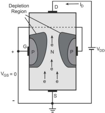
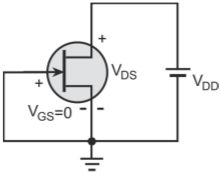
1. Positive drain-source voltage (VDS) with gate terminal shorted to the source terminal (VGS= 0).
Figure below shows the circuit connection.

n-channel JFET with VGS = 0 and positive value of VDS
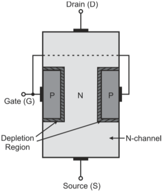
When positive drain-source voltage is applied, the electrons in the n-channel are attracted to the drain-terminal establishing the flow of drain current (ID). The value of ID depends on the value of the applied VDS and the resistance of the n-channel between the drain and the source terminals. Due to the flow of ID, there is a uniform voltage drop across the channel resistance. This reverse-biases the two P-N junctions and hence there is an increase in the width of the depletion region. Depletion region is wider near the drain-region than the source-region because ID and the channel resistance establish more reverse-bias voltage at the P-N junction near the drain-region as compared to that near the source-region.
n-channel JFET with VGS= 0 and positive value of VDS
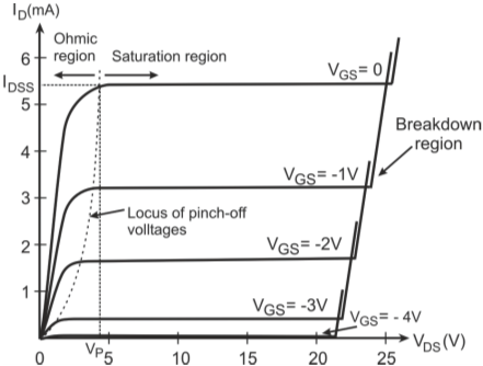
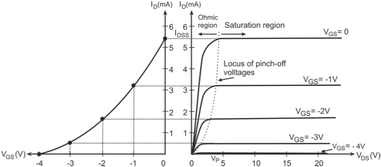
ID increases linearly with increase in VDS till the VDS reaches a value where the saturation effect sets in. This value of VDS where the saturation effect sets in is referred to as the pinch-off voltage (VP). After VDS equals VP, the value of ID does not change with further increase in the value of VDS. This condition is referred to as the pinch-off condition and the value of drain current is referred to as the drain-to-source current for short circuit connection between gate and source (IDSS). Figure below shows the ID versus VDSfor VGS = 0 curve.
ID versus VDS for VGS = 0
Pinch-off happens because the width of the depletion regions of the P-N junctions has increased significantly near the D-region resulting in reduction of the channel width as shown in figure below. Therefore, ID is equal to IDSS and essentially remains constant for VDS > VP. In nutshell, for VDS > VP, JFET has characteristics of a constant current source.
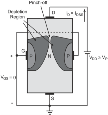
n-channel JFET with VGS = 0 and VDS VP
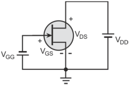
2. Both drain and gate voltages are applied to the JFET
For an n-channel JFET, negative VGS is applied to the FET, whereas for p-channel JFETs,VGS is positive. Figure below shows the circuit connection when both drain and gate voltages are applied to the JFET.
n-channel JFET biasing circuit
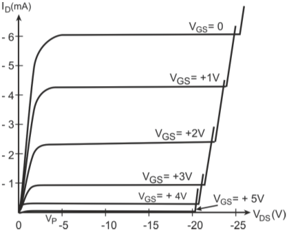
When a negative bias is applied to the gate terminal, it is reverse biased. Hence, there is an increase in the width of the depletion region. Therefore, the pinch-off phenomenon occurs at lower values of VDS and the value of saturation drain current decreases. As the value of VGS becomes more negative, the value of saturation current further decreases. The drain current becomes zero for VGS equal to –VP. This voltage is referred to as the gate-source cut-off voltage or the gate-source pinch-off voltage (VGS(off)). The value of drain-source pinch-off voltages decreases in a parabolic manner with theVGS becoming more negative.