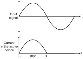
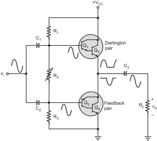
Let us assume that the output characteristics of the active device are equally spaced and also that the minimum collector current is zero. Figure below shows the graphical schematic for determining the output waveform of a single class B transistor stage. As we can see that for a sinusoidal input excitation, the output is sinusoidal during the first half of the input cycle and is zero during the second half cycle.
Output waveform of a single class B transistor stage
Where,
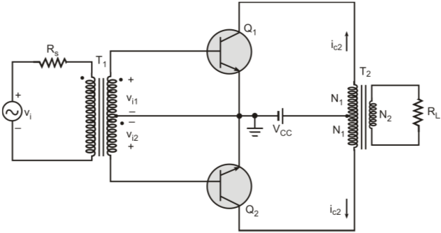
N1 is the number of primary turns to the center tap
N2 is the number of secondary turns
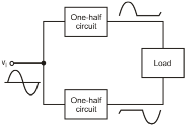
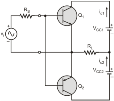
Figure below shows that the collector current waveforms of transistors Q1 and Q2.
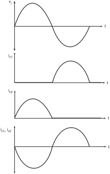
Output waveforms for class B push–pull amplifiers
As is clear from the figure, the output waveform of transistor Q2 is 1800
out-of-phase to that of transistor Q1. The load current is proportional to the difference
between the collector currents flowing through the transistors Q1 and Q2. It is therefore
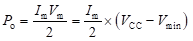
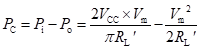
a perfect sine wave for ideal conditions. The output power (Po) is given by
The maximum power (Po(max)) that can be delivered to the load occurs for the
conditions Vm = VCC, Vmin = 0 and the operating
point is at the center of the output characteristics of the transistor.
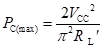
The value of Po(max) is given by
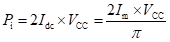
The DC input power (Pi) from the supply is given by
Where,
Idc is the DC value of the input current
The factor of 2 arises because the two transistors are used in push–pull configuration.
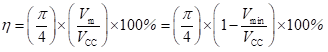
The efficiency of the circuit is given by
Therefore,
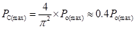
The efficiency is maximum when Vmin = 0. The maximum possible
conversion efficiency is equal to 25π which is equal to 78.5%. For practical systems,
the efficiency achieved is not as high as 78.5% but the value of efficiency is higher in
systems where the minimum value of the input signal is much less than the supply
voltage (i.e., Vmin << VCC).