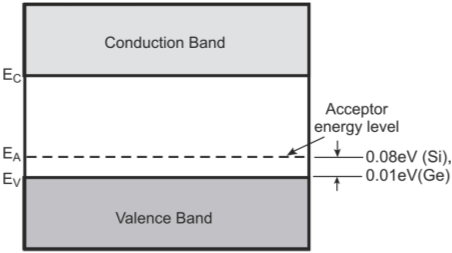
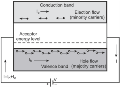
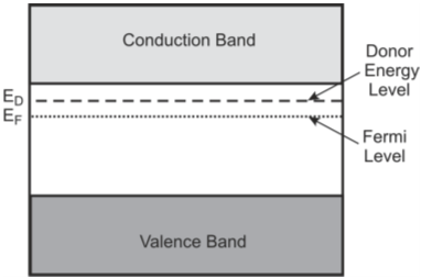
Figure below shows the Fermi level in a P-type semiconductor. The Fermi level in a P-type semiconductor is closer to the valence band and is lower than that of an intrinsic semiconductor. This is due to the fact that in a P-type semiconductor, there is a significant increase in the number of holes in the valence band and decrease in the number of electrons in the conduction band.
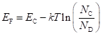
The expression for Fermi level (EF) in a P-type semiconductor is
Where,
EV is the energy at the top of the valence band
NV the density of states in the valence band (constant for a material at a given temperature)
T the temperature in Kelvin.
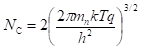
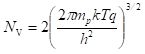
The value of NV is can be calculated using
Where,
mp is the effective mass of a hole
h the Plank’s constant
T the temperature in Kelvin
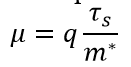
q the electronic charge (1.6 X 10⁻¹⁹ C)
k the Boltzmann constant in eV/°K (= 8.642X10⁻⁵ eV/°K)
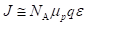
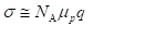
NA the donor atom concentration (number of atoms/cm3)
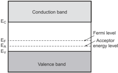
Fermi level in a P-type semiconductor