Intrinsic Semiconductors

  • What are intrinsic semiconductors? Give examples.

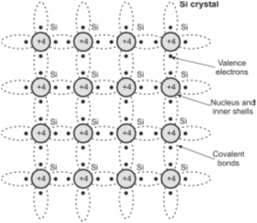
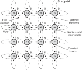
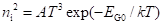
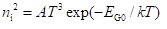
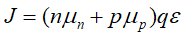
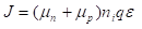
    Intrinsic semiconductors are semiconductors with very low level of impurity concentration. They have purity levels are of the order of 1 part in 10 billion. Examples of intrinsic semiconductors include Silicon, Germanium, Gallium Arsenide and Indium Antimonide.

  • What is the phenomenon behind conduction in intrinsic semiconductors?

    Conduction in intrinsic semiconductors is either due to thermal excitation or due to crystal defects.

  • Explain the crystal structure of Silicon at absolute zero temperature (0K)?

    Silicon has four valence electrons and is therefore referred to as a tetravalent atom. These four electrons are shared by four neighboring atoms in the crystal. Due to this sharing of four electrons of an atom with their respective neighboring atoms, this constitutes a total of eight electrons in its valence shell. This bonding of atoms due to sharing of electrons is called covalent bonding. Owing to the covalent bonding, the valence electrons are tightly bound to the nucleus resulting in poor conductivity of Silicon crystal at absolute zero temperature (0K) and low temperatures. Figure below shows the crystal structure of Silicon at absolute zero temperature (0K)

    Crystal structure of Silicon (Si) at absolute zero temperature (0K) and low temperatures

  • Explain the crystal structure of Silicon at room temperature (300K)?

    At room temperature (300K), the thermal energy of the atom is sufficient enough to break some of the covalent bonds. These electrons are raised to the conduction band and are referred to as free electrons. The free electrons are available for conduction. Figure below shows the crystal structure of Silicon at 300K.

    Crystal structure of Silicon (Si) at room temperature

  • How can we classify intrinsic semiconductors?

    Intrinsic semiconductors can be classified as
    - Direct band gap semiconductors
    - Indirect band gap semiconductors

  • What are direct band gap semiconductors?

    Direct band gap semiconductors have the maximum energy of the valence band at the same momentum value as the minimum energy of the conduction band. Figure below shows the energy-momentum diagram of a direct band gap semiconductor.

    Energy-momentum diagram of direct band gap intrinsic semiconductor

  • Give examples of direct band gap semiconductors?

    Examples of direct band gap semiconductors include Gallium Arsenide and Mercury Cadmium Telluride.

  • Why direct band gap semiconductor materials are used in construction of LEDs and laser diodes?

    In a direct band gap semiconductor, when electrons present at the minimum of conduction band combine with holes present at the maximum of valence band, the momentum is conserved. The energy released due this recombination is emitted in the form of photon of light. Hence, direct band gap semiconductors are used in making light-emitting diodes (LED) and laser diodes.

  • What are indirect band gap semiconductors?

    In an indirect band gap semiconductor, the maximum energy of the valence band occurs at a different momentum value than the minimum energy of the conduction band as shown in Figure below

    Energy-momentum diagram of indirect band gap intrinsic semiconductor

  • Give examples of indirect band gap semiconductors?

    Silicon and Germanium are examples of indirect band gap semiconductors.

  • How do indirect band gap semiconductor materials release energy?

    In indirect band gap semiconductors, direct transition of electrons and holes across the band gap does not conserve momentum and does not emit photons of light. Instead, the energy in this case is released in the form of heat.

  • Write the charge concentration equations for an intrinsic semiconductor?

    In an intrinsic semiconductor, the number of holes is equal to the number of electrons. Therefore,

    n=p=ni

    Where,
    n is the electron concentration (number of electrons/cm3)
    p is the hole concentration (number of holes/cm3)
    ni is the intrinsic concentration.

    The value of ni is given by

    Where,
    T is the temperature in Kelvin
    EG0 is the energy gap at 0K
    k is the Boltzmann constant in eV/K
    A is a constant

  • What is the relation between the intrinsic concentration ni and temperature?

    The value of ni is given by

    From the above equation, we can infer that the intrinsic concentration ni increases with increase in temperature.

  • Write the expression for drift current density in an intrinsic semiconductor.

    Drift Current density in any material is given by

    Where,
    J is the current density in Amp/cm2
    n is the electron concentration (number of electrons/cm3)
    p is the hole concentration (number of holes/cm3)
    μ is the mobility of an electron in the material in cm2/Vs
    μ is the mobility of a hole in the material in cm2/Vs
    q is the charge of an electron (1.6 × 10⁻¹⁹ C)
    ε is the applied electric field in V/cm

    Since in an intrinsic semiconductor, n = p = ni, therefore the drift current density in an intrinsic semiconductor is given by

  • Write the expression for conductivity in an intrinsic semiconductor.

    The expression for conductivity (&sigma) is given by

    Therefore, for an intrinsic semiconductor, the expression for conductivity is

  • Write the expressions for Energy Band Gap for Silicon and Germanium semiconductors?

    The energy band gap [EG(T)] for Silicon at temperature T (K) is given by

    The energy band gap [EG(T)] for Germanium temperature T (K) is given by

    Where,
    T is the temperature in Kelvin

  • Write the values of band gap energies for Silicon and Germanium at room temperature (300K)

    The values of band gap energies for Silicon and Germanium at room temperature (300K) are 1.1 and 0.72 eV, respectively.

  • How does the value of band gap energy change with temperature?

    The value of band gap energy decreases with increase in temperature.

  • Write the expression for Fermi–Dirac probability function in a semiconductor?

    The probability that an energy level (E) in a semiconductor is occupied by an electron is given by Fermi–Dirac probability function [f(E)]. The expression for this function is

    Where,
    k is the Boltzmann constant (8.642 × 10⁻⁵eV/℃K)
    T is the temperature in Kelvin
    EF is the Fermi level in eV

    It may be mentioned here that the expression for Fermi–Dirac probability function for an extrinsic semiconductor is same as that for the intrinsic semiconductor.

  • What is the Fermi level in an intrinsic semiconductor?

    In an intrinsic semiconductor at 0K, the probability of finding an electron in the valence band is 100% and the probability of finding the electron in the conduction band is 0%. Therefore, the Fermi level in an intrinsic semiconductor at 0K lies at the center of the forbidden band gap as shown in the figure below.

    Fermi–Dirac probability function of an intrinsic semiconductor at 0K

    As the temperature increases, some of the electrons are excited to higher energy levels and they leave the valence band and jump to the conduction band. Thus, the probability of finding an electron in the valence band decreases and the probability of finding an electron in the conduction band increases. The Fermi level still remains at the center of the forbidden band gap as shown in the Figure below.

    Fermi–Dirac probability function of an intrinsic semiconductor at 300K

  • Why do intrinsic semiconductors have limited applications?

    Intrinsic semiconductors have very limited applications as they conduct a very small amount of current.

  • How can we change the electrical characteristics of an intrinsic semiconductor material?

    The electrical characteristics of an intrinsic semiconductor are changed significantly by adding impurity atoms to the pure semiconductor material. The impurities added are of the order of 1 part in 105 parts to 1 part in 108 parts.

Got a voltage spike of curiosity?

Send your doubts now!