Semiconductor Fundamentals

  • What are semiconductors?

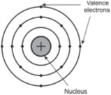
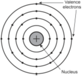
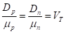
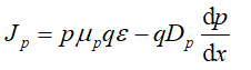
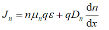
    Semiconductors are materials having resistivity levels in between that of conductors and insulators. Their resistivity levels are in the range of 10–104 Ωcm.

  • Name some commonly used semiconductor materials.

    Most commonly used semiconductor materials are Silicon (Si), Germanium (Ge), Gallium Arsenide (GaAs) and Indium Phosphide (InP)

  • Draw the atomic structure of Silicon.

    Figure below shows the atomic structure of Silicon. As we can see from the figure, Silicon has 14 orbiting electrons. Also, it has four valence electrons.

    Atomic structure of Silicon (Si)

  • Draw the atomic structure of Germanium.

    Figure below shows the atomic structure of Germanium. As we can see from the figure, Germanium has 32 orbiting electrons. Also, it has four valence electrons.

    Atomic structure of Germanium

  • Draw the energy band structure of semiconductors.

    Figure below shows the energy band structure of semiconductors. As we can see from the figure, forbidden energy gap in case of semiconductors is of the order of 1 eV.

    Energy band diagram of a semiconductor

  • What are the band gap energy levels for Silicon, Germanium and Gallium Arsenide at absolute zero temperature (0K)?

    At 0K, the band gap energy levels are as follows
    - Silicon : 1.21eV
    - Germanium : 0.785eV
    - Gallium Arsenide : 1.42 eV

  • What is the effect of temperature on the conductivity levels of a semiconductor?

    At absolute zero (0K) and low temperatures, valence band electrons do not have sufficient energy to cross the energy band gap and reach the conduction band. Therefore, at these temperatures, semiconductors act as insulators.

    As the temperature increases, a large number of valence electrons acquire sufficient energy to leave the valence band, cross the energy band gap and reach the conduction band. These are now free electrons as they can move freely under the influence of an external applied electric field. At room temperature (300K), there are sufficient electrons in the conduction band. Therefore, the semiconductor is capable of conducting some current at room temperature. Hence, the conductivity of a semiconductor increases with increase in temperature.

  • What is a hole?

    The absence of an electron in the valence band of an atom is referred to as a hole and is represented by a small hollow circle. Hole has a positive charge and serves as a carrier of electricity in a manner similar to electrons. In fact, the motion of hole in one direction is equivalent to the motion of electron (negative charge) in the opposite direction.

  • What constitutes the flow of current in a semiconductor?

    Both electrons and holes constitute the flow of current in a semiconductor.

  • Why is semiconductor referred to as a bipolar device?

    A semiconductor is referred to as a bipolar device as both electrons and holes contribute to the flow of current. There are two different mechanisms of current flow in a semiconductor, namely, the ‘electron flow in the conduction band’ and the ‘hole flow in the valence band’.

  • What is drift current and drift velocity?

    Drift current in any material is the current is due to the potential gradient in the material when an electric field is applied across it.

    When an electric field is applied across the semiconductor material, the charge carriers attain a certain drift velocity (Vd). This drift velocity is expressed as

    Where,
    μ is the mobility of the charge carrier
    E is the applied electric field intensity

  • What is diffusion current?

    Diffusion currents are present only in semiconductors. Diffusion current is caused by the concentration gradient in the semiconductor, that is, when there is non-uniform concentration of charge particles in a semiconductor.

  • Write the expressions for hole and electron diffusion current density in a semiconductor.

    The hole diffusion current density is given by the expression

    Where,
    Dpis the diffusion constant of holes in cm2/s dp/dx the variation in hole concentration with distance x (it is positive when the hole concentration increases with distance and is negative if the hole concentration decreases with distance)

    The electron diffusion current density is given by the expression

    Where,
    D n is the diffusion constant of electrons in cm 2 /s
    dn/dx is the variation of electron concentration with distance x (it is positive when the concentration of electrons increases with distance and is negative if the concentration of electrons decreases with distance)

  • What is the relation between the diffusion constant of a carrier and its mobility?

    The diffusion constant of a carrier is related to its mobility and is given by

    Where,
    V T is the volt equivalent of temperature, and is equal to kT (k is the Boltzmann constant in eV/°k and T is the temperature in Kelvin)

  • Write the expression for the total hole and electron current density in a semiconductor?

    The total hole current density is given by the expression

    The total electron current density is given by the expression

  • How do we define Fermi level in a semiconductor?

    Fermi level represents the energy state with 50% probability of being filled by an electron if no forbidden energy band gap exists.

Got a voltage spike of curiosity?

Send your doubts now!