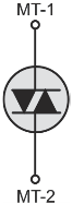
A DIAC is a bi-directional thyristor. It can be considered to be equivalent to two PNPN devices connected back-to-back as shown in figure below.
DIAC construction
A DIAC is a bi-directional thyristor. It can be considered to be equivalent to two PNPN devices connected back-to-back as shown in figure below.
DIAC construction
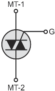
Figure below shows the circuit symbol of a DIAC. As we can see from the figure, it is a two-terminal device with the terminals designated as MT-1 and MT-2.
DIAC circuit symbol
Figure below shows the V-I characteristics of a DIAC. As we can see from the figure, V–I characteristics of a DIAC are similar to those of a four-layer PNPN diode with the difference that a DIAC exhibits identical characteristics both in the forward (first quadrant) and reverse (third quadrant) directions.
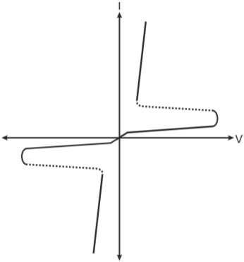
V-I characteristics of a DIAC
A TRIAC is equivalent to a DAIC with a gate contact. It is a three-terminal device and the terminals are designated as Main Terminal-1 (MT-1), Main Terminal-2 (MT-2) and Gate.
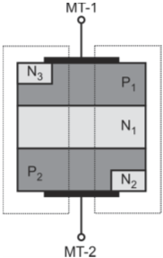
Figure below shows the construction of a TRIAC.
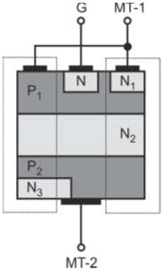
Construction cross-section of a TRIAC
Figure below shows the V-I characteristics of a TRIAC.
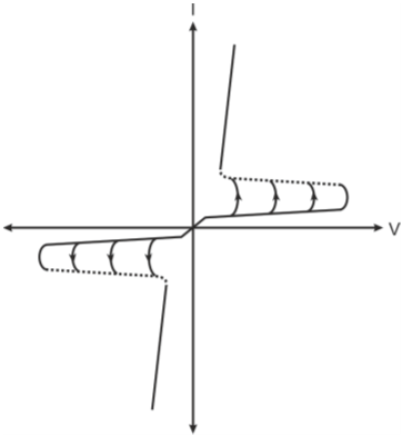
V-I characteristics of a TRIAC
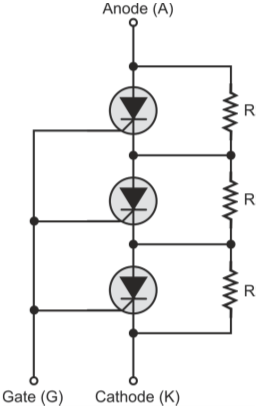
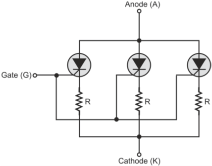
Silicon bilateral switch (SBS) is a device similar to TRIAC in construction, but without the gate terminal. Its characteristics are symmetrical and it switches ON and breaks down for applied voltage of both polarities.
Major performance specifications of a thyristor are listed below • Repetitive peak reverse voltage, VRRM • Non-repetitive peak reverse voltage, VRSM • Repetitive peak OFF-state voltage, VDRM • Break-over voltage, VBO • Critical rate of rise of ON-state current (di/dt) • Critical rate of rise of OFF-state voltage (dv/dt) • Holding current, IH • Holding voltage, VH • Latching current, IL • I2t rating Figure below shows the V-I characteristics of a thyristor listing various performance parameters of a thyristor.
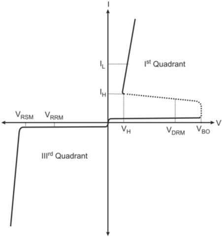
Thyristor parameters
Repetitive peak reverse voltage (VRRMs is defined for reverse-blocking mode of thyristors like SCRs for operation in the third quadrant of the V-I characteristics. It is the maximum repetitive reverse voltage (anode negative with respect to the cathode) that can be applied to the device safely while still keeping it in the blocked state. The current that flows through the device in this state is referred to as the repetitive peak reverse current (IRRM).
Non-repetitive peak reverse voltage is also defined in a similar way as for repetitive peak reverse voltage. Non-repetitive peak reverse voltage rating of a thyristor is a little higher than repetitive peak reverse voltage.
Repetitive peak OFF-state voltage (VDRM) is the maximum forward OFF-state voltage (anode positive with respect to cathode) that can be allowed to appear across the device when it is being operated in the first quadrant (in the forward-blocking mode). Repetitive peak OFF-state voltage (VDRM) is much less than the actual break-over voltage (VBO) of the device and applied voltage should not exceed VDRM so that the device retains its listed characteristics. The maximum value of current that can flow in the forward-blocking state is designated as IDRM.
Break-over voltage (VBO) or peak OFF-state voltage (VDM) is the maximum OFF-state voltage. If the applied forward voltage were greater than the break-over voltage, the device is switched to the ON-state even in the absence of any gate signal. It does not depend upon the voltage grades of different thyristors in the same family.
When a thyristor is switched ON, initially, the thyristor can handle a very small current as it is concentrated in a small area of the device pellet. Gradually, the load-current-carrying capability increases to its specified rating. Critical rate-of-rise of ON-state current (di/dt) tells us about the maximum rate of change of ON-state current the device can handle safely. If this rating is exceeded during device switch ON there could be a development of localized hot spots in the pellet at the time of switch ON and this could result in the device getting damaged. di/dt rating of 100 A/s is typical.
The critical rate of rise of OFF-state voltage (dv/dt) determines the maximum allowable rate of change of applied forward OFF-state voltage. When a time-varying applied forward voltage is applied to a thyristor, a current equal to C × dv/dt flows through the reverse-biased junction capacitance (C) of the thyristor. This current if more than a certain value can cause premature firing of the thyristor due to decrease in its break-over voltage. Maintaining dv/dt within dv/dt rating of the device ensures that there is no change in the break-over voltage (VBO) of the device. A dv/dt rating of 100 V/µs is quite common.
Holding current (IH) and holding voltage (VH) are defined when the thyristor is in the ON-state and has to be kept there only. When the voltage across the thyristor is decreased so that the current decreases, then at a particular stage, the current is not able to keep the device in the ON-state. So, the device goes to OFF-state. Holding current is minimum ON-state current required to keep the thyristor in the low impedance state once it has been triggered to the ON-state. In order to switch off the thyristor, the anode current must be brought below the holding current value. Voltage corresponding to holding current is termed as “holding voltage”.
Latching current (IL) is little larger than the holding current. ON-state current equal to or more than the latching current ensures that once the thyristor is switched ON, it remains in the ON-state even after the gate signal is removed. Once the ON-state current has exceeded the latching current value after switch ON, the current then has to be brought below the holding current to switch it OFF.
The amperes squared seconds (I2t) rating of a thyristor tells us about the surge current-handling capability of the device for sub-cycle time periods when the device is being used as a rectifier. I2t rating of the thyristors can be used to calculate the surge current capability when the thyristor conducts for only a part of the full cycle time period.
Thyristors are current-controllable devices because their V–I characteristics can be expressed by a single-valued function of current. That is, for every current value, there is one and only one corresponding voltage value. On the other hand, these characteristics are representative of a multi-valued function of voltage. It is because of “single-valued function of current” and “multi-valued function of voltage” nature of the V–I characteristics that thyristors are considered as current-controllable devices. UJTs also belong to the same class.
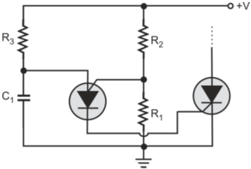
While connecting thyristors in series, steps should be taken to ensure that the applied voltage is equally divided between the individual devices. The devices connected in series should preferably have closely matched OFF-state characteristics like forward break-over voltage, OFF-state resistance and so on. One way to force an equal division amongst individual thyristors is to connect identical resistors across each one of the thyristors connected in series as shown in figure below. The value of R should be a fraction of the forward OFF-state resistance. This will ensure that that any variation in OFF-state resistance from device to device does not affect the voltage division. Capacitive dividers are also used as the resistors dissipate power and reduce the efficiency. In the case of capacitive dividers, a series resistance should be used alongwith each capacitor to damp the current pulses.
Thyristors in series
The total ON-state current should be equally divided amongst individual thyristors connected in parallel. To achieve this, the thyristors should preferably have closely matched forward conduction characteristics like the ON-state dynamic impedance, ON-state voltage and so on. Equal division of current can be forced by connecting small resistors in series with each of the parallel connected thyristors (as shown in figure below). R in this case is much larger than the ON-state dynamic impedance of the individual thyristors.
Thyristors in parallel
Figure below shows the use of an SCR in a pulse generator circuit.
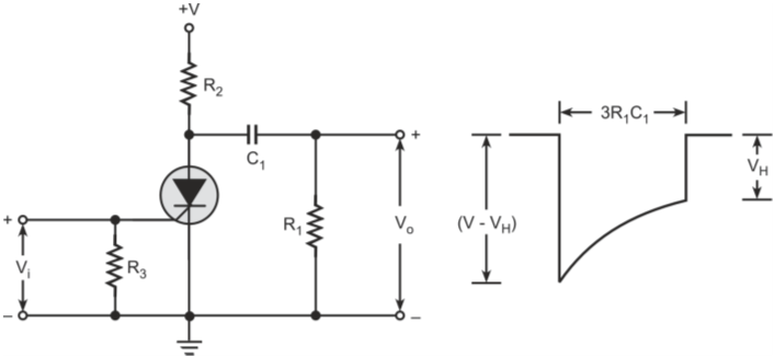
SCR-based pulse generator
In the normal state, the output voltage is at ground level as the capacitor C1 is charged to V volts. The break-over voltage of the SCR used in the circuit must be greater than the voltage V. When a trigger pulse is applied at the gate of the SCR, it fires and the voltage across SCR tends to change abruptly to VH from V changing by V VH. Capacitor C1 discharges through the ON resistance (r) of the SCR and resistance R1. Generally, r < R1, therefore the discharging time constant is R1C1. The capacitor discharges only upto a voltage VH (called holding voltage). This is so because beyond that holding current of the SCR can no longer be supplied and the SCR turns-OFF. Since, voltage across a capacitor cannot change abruptly, the output voltage (VO) changes abruptly from 0 to –(V VH) and then rises exponentially as C1 discharges. The output abruptly goes to zero when voltage across C1 has decayed to VH which can no longer supply the holding current (IH). The output pulse-width in this case is about 3R1C1.
Figure below shows the basic circuit arrangement of a bistable multi-vibrator using SCRs.
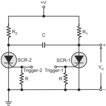
SCR-based bistable multi-vibrator
The circuit can be used as a bistable multi-vibrator if the supply voltage is less than the break-over voltage of the SCRs. Assume that SCR-1 is initially conducting and SCR-2 is in cut-off. Under these conditions, the current flowing through SCR-1 is limited by R1 only and the output voltage is low (= VH). R1 is chosen in such a way that current through SCR-1 is only slightly greater than the holding current. If we apply a positive trigger at the gate of SCR-2, it starts conducting and the anode voltage of SCR-2 drops from V to VH. This abrupt change is transmitted to the anode of SCR-1 as voltage across C cannot change instantaneously. This negative-going step at SCR-1 anode, turns it OFF. Also, the current that flows through C as a result of SCR-2 anode going to an almost zero potential has to be supplied through R1. R1 cannot supply both the holding current for SCR-1 as well as current through C. As a result, current through SCR-1 falls below its holding current value and is turned-OFF. As SCR-1 goes to OFF-state, output goes high (= V). A positive trigger at SCR-1 gate again changes state.
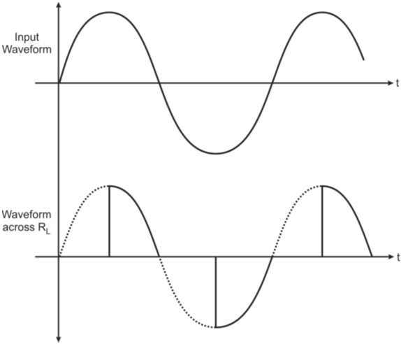
Circuit diagram of a SCR based half-wave controlled rectifier is shown in figure below. During the positive half cycle of the AC source, circuit in the box labelled ‘phase control’, controls the point at which the gate-trigger pulse is applied to the SCR gate. During the negative half cycle, SCR remains reverse-biased and there is no current through the load. Therefore, input AC power appears across the load only during the conduction period of the SCR. The AC power in the load thus can be controlled by controlling the firing angle of SCR. The firing angle can be anywhere between 0º and 180º.
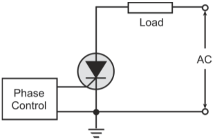
SCR based half-wave controlled rectifier
Figure below shows the waveform appearing across the load.
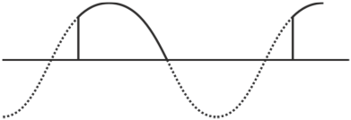
Load waveform
Figure below shows the SCR anode waveform.
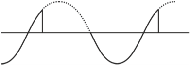
SCR anode waveform
Figure below shows the circuit of a SCR based full-wave controlled rectifier
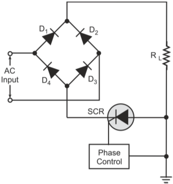
SCR based full-wave controlled rectifier
Conduction angle is 90º. Diodes D1 and D3 conduct during positive half cycles of input whereas diodes D2 and D4 conduct during negative half cycles of input. The power control is provided by SCR. Figure below shows the input and output waveforms.
Relevant waveforms in full-wave controlled rectifier
An SCR-based crowbar circuit protects the output voltage of a power supply from becoming excessively high. Figure below shows the SCR-based crowbar protection circuit.
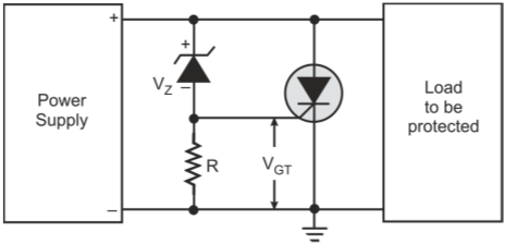
SCR-based crowbar protection circuit
The over-voltage at which crowbar action occurs is given by (VZ + VGT). VZ is selected to be higher than the normal operating voltage of the power supply. The crowbar circuit remains inactive as long as the power supply output voltage is less than (VZ + VGT). If the output voltage exceeds (VZ + VGT), SCR is triggered. It shorts the load, thus protecting the load from excessive voltage. Crowbar is always used in conjunction with a fuse or some kind of current limiting to protect the power supply.
Turn-ON time is an important parameter of a crowbar circuit. SCRs with turn-ON time as fast as a microsecond suit the application.
The turn-on of SCR in the circuit above is dependent on the breakdown of the Zener diode. Owing to a slightly curved knee at the breakdown point in the Zener V-I characteristics, the device becomes a bit sluggish. Therefore, the response of the crowbar circuit is sluggish.
Figure below shows the circuit of TRIAC-based AC power control circuit. Here the phase angle is being controlled by a DIAC. During both positive and negative half cycles, the TRIAC conducts as and when the break-over voltage of the DIAC is exceeded. The TRIAC turns-OFF when the current falls below its holding value. Another trigger during the negative half cycle turns the TRIAC on again. The period for which the TRIAC conducts during positive and negative half cycles of AC input can be controlled by varying R. By controlling time constant (RC), we can control the time instant at which DIAC would fire which in turn triggers the TRIAC.
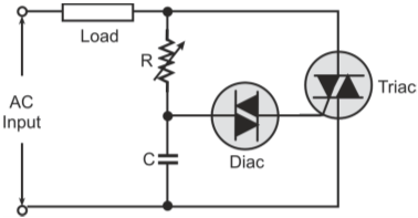
TRIAC-based AC power control
Gate turn-OFF thyristors (GTO) are special type of thyristors, which can be switched to the ON and OFF states by applying appropriate trigger pulses to the gate terminal.
A GTO can be turned ON by a positive current pulse applied between gate and cathode terminals. However, the turn-ON phenomenon in a GTO is not as reliable as it is in the case of a conventional thyristor. A small magnitude of positive gate current is therefore maintained even after turn-ON to improve reliability.
GTO can be turned OFF by applying a suitable negative voltage pulse. Application of negative voltage initiates a reduction in the forward current by about 20–30%. This reduction in forward current induces a cathode-to-gate voltage which further reduces the forward current. The process ultimately culminates in the device transitioning to the blocking state.
As compared to conventional thyristors, GTO thyristors have relatively higher ON-state voltage drop, longer turn-ON and turn-OFF times and also require higher turn-ON gate current.
GTO thyristors can be classified as asymmetrical GTO thyristors (A-GTO) and symmetrical GTO thyristors (S-GTO). GTO thyristors without reverse-blocking capability are known as asymmetrical GTO thyristors whereas GTO thyristors with reverse-blocking capability are known as symmetrical GTO thyristors.
Major application areas of GTO thyristors include their use in variable speed motor drives, high power inverters and traction.
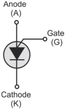
PUT is a four-layer device like a thyristor with contacts, namely, anode (A) and cathode (K) made to the two extreme layers and a control contact called gate (G) made to one of the inner layers. In this case, the inner layer chosen is the one closer to the anode contact. The device is so called because it can perform functions similar to that of a UJT and is directly interchangeable with a UJT device.
Most common application UJT and PUT devices is in triggering of thyristors. Figure below shows the triggering of thyristor using a PUT device
Thyristor triggering with a PUT device