Transistor Biasing Basics

  • What is transistor biasing?

    In order to establish a proper operating point for the transistor [collector current (IC) and collector–emitter voltage (VCE)], external components such as resistors and capacitors are used and DC voltages are applied to the transistor. This process is referred to as transistor biasing

  • What is a basing circuit?

    Circuit used for transistor biasing is called a biasing circuit.

  • What conditions should be met for a transistor to act as a faithful amplifier?

    There are four conditions that should be met for a transistor to act as a faithful amplifier.

    • The emitter-base junction should be forward-biased and the collector-base junction should be reverse-biased for all levels of input signal.
    • The collector–emitter voltage (VCE) should not fall below the knee voltage (VCE(sat) for any part of the input signal, otherwise the collector–base junction is not properly reverse-biased.
    • The value of collector current (IC) when no signal is applied should be at least equal to the maximum collector current due to signal alone.
    • The maximum ratings of the transistor (IC(max), VCE(max) and PD(max)) should not be exceeded at any value of the input signal.

  • What is an operating point?

    The DC collector current (IC) and the collector–emitter voltage (VCE) when no input signal is applied is referred to as the operating point.

  • Why is the operating point also referred to as the quiescent point?

    The operating point is referred to as the quiescent point (Q-point) as it is a fixed point on the output characteristics of the transistor.

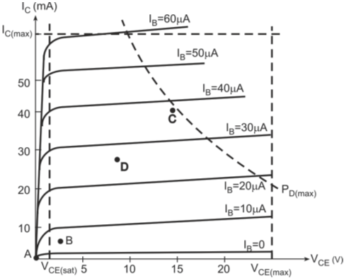
  • Refer to the figure below. It shows the output characteristics of a common-emitter amplifier with four different operating points. Which point is best suitable for faithful amplification of the input signal?

    Point D is located in the middle of the active region of the transistor characteristics. It will provide maximum linear gain and largest possible output voltage and current swing. It is the best suitable operating point.

    Output characteristics with different operating points

    Operating point A drives the transistor in the cut-off region. Point B would allow some positive and negative variations of the output signal but the peak-to-peak output voltage is limited due to the proximity of the operating point to the knee point (VCE(sat)). Point C is too close to the PD(max) curve of the transistor. Therefore, the output voltage swing in the positive direction is limited. Therefore, operating points A, B and C are not suitable.

  • What do you mean by DC analysis?

    DC analysis of a circuit refers to analyzing a circuit so as to establish the operating point in the absence of any input AC signal. For the purpose of DC analysis, the input and output capacitors are considered as open and it is assumed that all AC sources are zero.

Got a voltage spike of curiosity?

Send your doubts now!