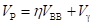
Figure below shows the basic UJT-based relaxation oscillator circuit.
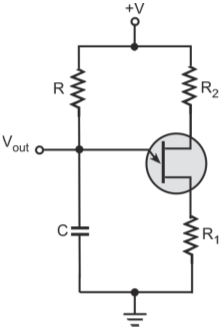
UJT relaxation oscillator circuit
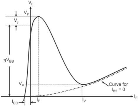
Initially UJT is in the cut-off region. The capacitor starts charging from voltage +V through resistor R. When the voltage Vout across the capacitor becomes large enough to forward bias the input diode, the capacitor starts discharging through the low resistance between the emitter-base B1 region and resistor R1. This discharge process continues until it reaches a point where input diode is again reverse-biased. At this point, the capacitor starts charging again. The process of charging through R, which is comparatively a higher resistance, and discharging through low forward resistance of input diode and R1 continues and gives rise to a waveform as shown in Figure below
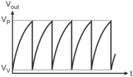
Waveform across the capacitor in basic UJT relaxation oscillator
The frequency of oscillation is given by
If we replace the resistor R with a constant current source (refer to figure below) then the voltage across the capacitor will be a sawtooth waveform.
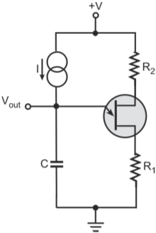
Constant current charging in UJT relaxation circuit
The sawtooth waveform is shown in figure below.
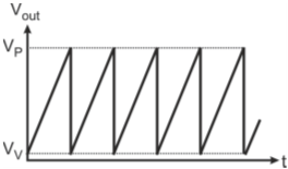
Waveform across the capacitor in UJT relaxation oscillator having constant current source
During the time UJT is ON, a train of positive pulses appear at B1 and a train of negative pulses appear at B2 as shown in figures below.
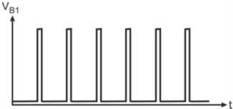
Waveforms at B1 terminal
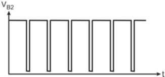
waveforms at B2 terminal
It may be mentioned here that UJT is no longer a popular device for building oscillators. It has been largely replaced by opamp- and timer IC-based circuits