Figure below shows the internal schematic of timer IC 555.
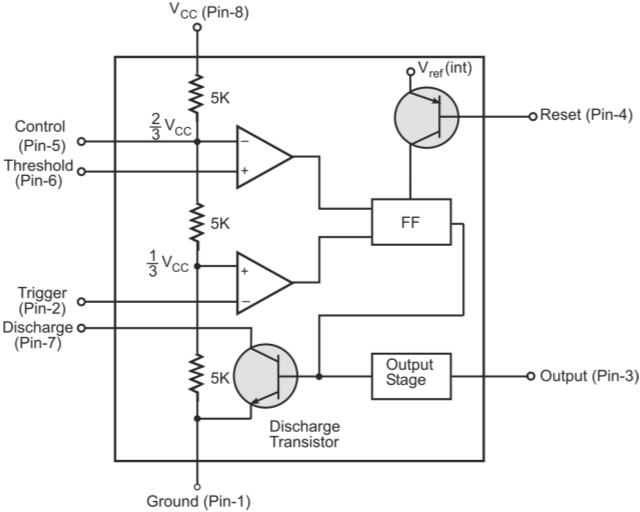
Internal schematic of timer IC 555
Different terminals of the timer 555 are designated as Ground (Terminal-1), Trigger (Terminal-2), Output (Terminal-3), Reset (Terminal-4), Control (Terminal-5), Threshold (Terminal-6), Discharge (Terminal-7) and +Vcc (Terminal-8).
Internally, it comprises two op-amp comparators, a flip-flop, a discharge transistor, three identical resistors and an output stage. The resistors set the reference voltage levels at the non-inverting input of the lower comparator and inverting input of the upper comparator at +VCC/3 and +2VCC/3, respectively. Outputs of two comparators feed SET and RESET input of the flip-flop and thus decide the logic status of its output and subsequently the final output. The flip-flop’s complementary outputs feed the output stage and the base of the discharge transistor. This ensures that when the output is HIGH, the discharge transistor is OFF and when the output is LOW, the discharge transistor is ON. With this background, we will now describe the astable and monostable circuits configured around timer 555.